
nX-FM1
Wafer Shape Measurement Equipment
The wafer warpage measurement system performs high-speed scanning to measure the entire shape of a 12-inch wafer in just 5 seconds. It is a process-reference equipment that provides full-surface shape data and 3D images at a high throughput level for process control in Advanced Wafer-Level Packaging (AWLP).
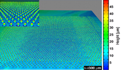
This system is capable of measuring wafers with significant warpage, which was challenging with conventional methods. It supports shape measurement for various types of wafers, including bare wafers, patterned wafers, bonded wafers, and glass wafers. The resulting comprehensive wafer data, along with high-resolution 3D images and analysis, will serve as crucial process data to enhance yield.
Application

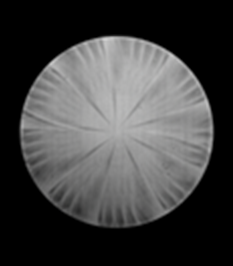
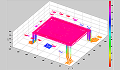
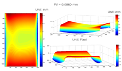
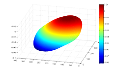
Wafer Warpage 3D Image

Wafer Warpage 3D Image
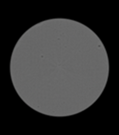
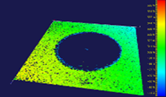
Wafer Warpage 2D Image
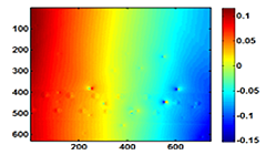
Wafer Wheel Mark 2D Image
Specifications
Request a specification
Contact us
Latest News


Request a sample test
Request a sample test now!
You can experience the technology of Nexensor.
You can experience the technology of Nexensor.
Contact us
| Measuring model | Measuring technology | Test content | Measuring data |

|
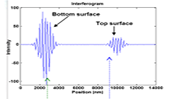
Large-area measurement with WSI interferometers FOV extensive application | Micro Bump Height Monolayer membrane thickness measurement PCB fine pattern Processed surface roughness measurement Sensor step-difference measurement |

|
|
Free-Form Metrology
Divided inspection possible according to product curve angels
|
Inspection of lens and glass, and measurement of shapes
Inspection of OLED surfaces, and measurement of shapes
Inspection of wafer surfaces, and measurement of shapes
|

|

|
Real-time measurement of transparent and semitransparent product thickness
Applicable to multi-channels
|
Measurement of wafer(silicone, sapphire) thickness
Measurement of glass and film thickness
|
|